Initial start of Cadence
Perform the following three commands once:
mkdir cadence61_tsmc90nmlp_oa
cd cadence61_tsmc90nmlp_oa
/projects/nanos/script/TSMC90NMLPRF_OA/init
This create a folder for Cadence and copy some files. Now go to the folder ./Calibre/drc and open the file calibre.drc in a text editor. Locate the line that defines FULL CHIP and comment it with a double dash.
//#DEFINE FULL_CHIP // Turn on by default
Fix a path in the pex rule file. Execute the following command from your cadence directory:
patch -p0 /projects/nano/kurs/INF4420/setup/calibre_rcx_pathfix.patch
Start Cadence in your Cadence folder with:
cd cadence61_tsmc90nmlp_oa
source CRN90LP_session
virtuoso&
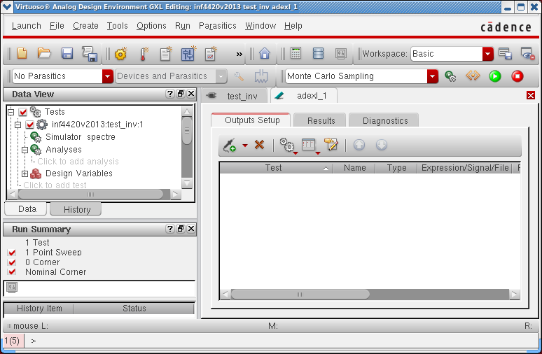
Simulation
Open the schematic or config cellview of the testbench. In the Virtuoso Schematic Editor windows, select Launch->ADE GXL. Hit OK in the next two dialog windows.
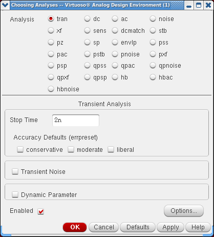
In the Data View pane, you can now "Click to add analysis". Select a tran(sient) simulation and set stop time to 2n(s) like this:
Hit OK. Add a signal by clicking the "probe" button. Click in the Expression/Signal/File twice. Type the name of the signal or use the browse button (...) to select the signal from the schematic. Repeat for all signals. If you click a terminal in the schematic, you will select the current in/out of that terminal. Select "Single Run, Sweep and Corners" or "Monte Carlo Sampling" from the drop down box.
When you run a Monte Carlo simulation, click the button to the right of the drop down box and check "Save Data to Allow Family Plots". If you don't, the simulator will not save any for plots.
If you double click the test, in this case called "inf4420v2013:test_inv:1", a window pops up:
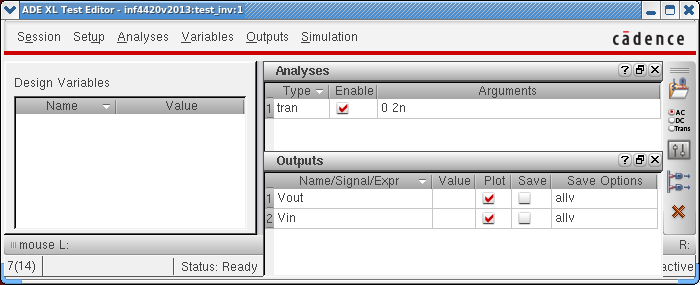
This window has more functions.
Outputs->Save All opens a dialog with which you can select which signals, currents and powers you will want to inspect once the simulation has finished. This is useful for "over night" and "all week" simulations.
Simulation->Convergence Aids->Initial Condition lets you set initial voltages on nodes.
Layout
An inverter is used as an example.
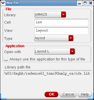
Start with an empty layout. Select the cell for layout and File->New->Cell View in the Library Manager and a dialog window will pop up. Chang Type to Layout and hit OK.
Now a window with a blank black layout sheet appears.
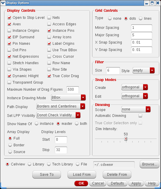
You need to change some options. Select Options->Display. Enable Pin Names and Instande Pins. Change X and Y Snap Spacing to 0.01 or 0.005. Change Display Levels Stop to 32 like this:
Create->Instance, Browse to Library: tsmcN90rf and select Cell: pch and View: layout. Place the transistor on the layout sheet.
In the LSW window, select layer: NW dra and Create->Shape->Rectangle. Now draw a new nwell large enough to house the transistor and the nwell strap you are going to create next.
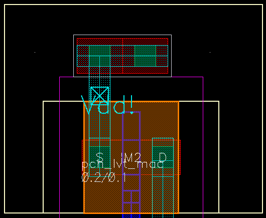
The nwell strap is not premade in version 6.
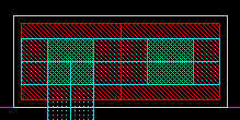
Start with a rectangle of "CO dg". This has to be exactly 0.12x0.12µm and is the green square. Around it, draw a red rectangle of "OD dg" a least 0.2x0.2µm. I have made it 0.26µm wide. Then I can place them side by side in a row like shown above. A metal1 path on top connects the vias to vdd and to the PMOS transistors. Now the nwell strap is finished and can be placed in the nwell. A rectangle of "NP dg" should extend the red OD by at least 0.02µm.
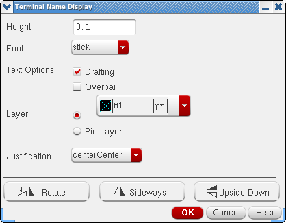
Now for the pins: Create->Pin. Write the name of the pin. Vdd and gnd should have an '!' at the end. Check Display Terminal Name. Select I/O Type and press the Display Terminal Name Option button. A Height = 1 is far too big. 0.1 is much better. Change Layer to M1 pn. Hit OK.
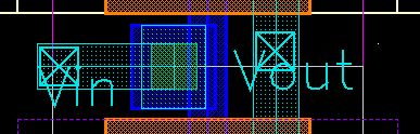
In the LSW window, select M1 pin. For each pin, type the Pin Name and draw a rectangle you can see and click once more for the pin name.
Now add an nch the same way as the pch an a substrate strap.
The substrate strap is made the same way as the nwell strap but with the "NP dg" replaced by a "PP dg" .
DRC (Design Rules Check)
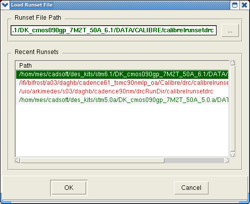
In the Virtuoso Layout window, select Calibre->Run DRC. Make sure the Runset File Path is:
/hom/mes/cadsoft/des_kits/stm6.1/DK_cmos090gp_7M2T_50A_6.1/DATA/CALIBRE/calibreIrunsetdrc
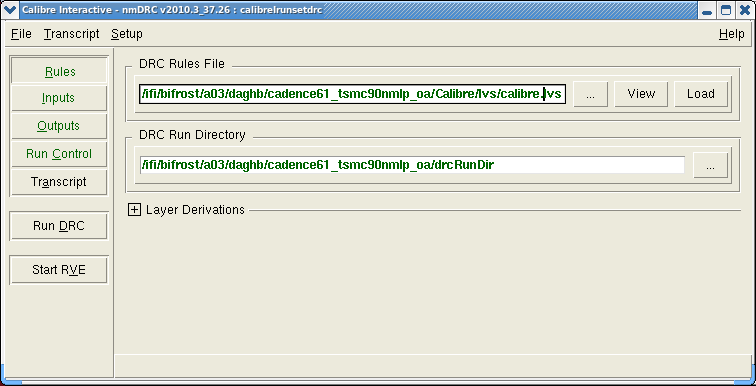
Hit OK. In the Calibre Interactive window press the Rules button.

Using the (...) button, browse to cadence61_tsmc90nmlp_oa/Calibre/drc/ and select calibre.drc. Hit OK.
Now hit the Run DRC button. A couple of report windows will appear telling you which checks have failed. Correct and run again until all checks have passed.
LVS (Layout Versus Schematic)
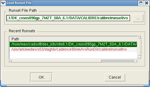
In the Virtuoso Layout window, select Calibre->Run LVS. Make sure the Runset File Path is:
/hom/mes/cadsoft/des_kits/stm6.1/DK_cmos090gp_7M2T_50A_6.1/DATA/CALIBRE/calibreIrunsetdrc
Hit OK. In the Calibre Interactive window press the Rules button.
Using the (...) button, browse to cadence61_tsmc90nmlp_oa/Calibre/lvs/ and select calibre.lvs. Hit OK.
Now hit the Run LVS button. Again a couple of report windows will appear telling you which checks have failed. Correct and run again until all checks have passed.
PEX (Parasitic EXtraction) and Post Layout Simulation
A pdf document showing the procedure using Cadence version 5: /studier/emner/matnat/ifi/INF4420/v12/PostLayoutTutorialTSMC90nm.pdf
In the "Calibre View Setup" dialog, replace the cellmap file "./calview.cellmap" with "./Calibre/rcx/calview.cellmap" .